
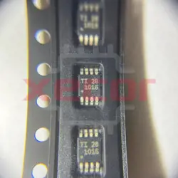
INA300AQDGSRQ1
Comparator Single 5.5V Automotive AEC-Q100 10-Pin VSSOP T/R
在庫:8,988
- 90日間のアフター保証
- 365日の品質保証
- 正規品保証
- 7*24時間サービス検疫
-
部品番号 : INA300AQDGSRQ1
-
パッケージ/ケース : VSSOP-10
-
ブランド : TI
-
コンポーネントのカテゴリ : Analog current-sense amplifiers
-
日付シート : INA300AQDGSRQ1 データシート (PDF)
概要 INA300AQDGSRQ1
The INA300-Q1 is a high common-mode, current-sensing comparator that detects overcurrent conditions by measuring the voltage developed across a current-sensing or shunt resistor. The device measures this differential voltage signal on common-mode voltages that can vary from 0 V up to 36 V, independent of the supply voltage. The INA300-Q1 device features an adjustable threshold range that is set using a single external limit-setting resistor. A selectable hysteresis feature enables adjustable operation of the comparator to accommodate the wide input signal range of 0 mV to 250 mV.
An open-drain alert output on the device can be configured to operate in either a transparent mode where the output status follows the input state, or in a latched mode where the alert output is cleared when the latch is cleared. The device response time setting is selectable, which enables overcurrent alerts to be issued in as fast as 10 µs.
The INA300-Q1 device operates from a single 2.7-V to 5.5-V supply, drawing a maximum supply current of 135 µA. The INA300-Q1 device is specified over the extended operating temperature range of –40°C to +125°C, and is available in a VSSOP-10 package.
主な特長
- Qualified for Automotive Applications
- AEC-Q100 Qualified With the Following Results:
- Device Temperature Grade 1: –40°C to +125°C Ambient Operating Temperature
- Device HBM ESD Classification Level 2
- Device CDM ESD Classification Level C6
- Functional Safety-Capable
- Documentation available to aid functional safety system design
- Wide Common-Mode Range: 0 V to 36 V
- Selectable Response Times:
- 10 µs, 50 µs, 100 µs
- Programmable Threshold:
- Adjust Using Single Resistor
- Programmable From 0 mV to 250 mV
- Accuracy:
- Offset Voltage: ±500 µV (Maximum)
- Offset Voltage Drift: 0.5 µV/°C (Maximum)
- Selectable Hysteresis:
- 2 mV, 4 mV, 8 mV
- Active Quiescent Current: 135 µA (Maximum)
- Selectable Disable Mode
- Disabled Quiescent Current: 3.5 µA (Maximum)
- Disabled Input Bias Current: 500 nA (Maximum)
- Open-Drain Output With Latch Mode Available
仕様
以下は、選択された部品の特性やカテゴリーに関する基本的なパラメータである。
| Product type | Analog output with integrated comparator | Common-mode voltage (max) (V) | 36 |
| Common-mode voltage (min) (V) | 0 | Input offset (±) (max) (µV) | 650 |
| Input offset drift (±) (typ) (µV/°C) | 0.1 | CMRR (min) (dB) | 96 |
| Supply voltage (max) (V) | 5.5 | Supply voltage (min) (V) | 2.7 |
| Iq (max) (mA) | 0.135 | Number of channels | 1 |
| Comparators (#) | 1 | Features | Alert Function, Low-side Capable |
| Rating | Automotive | TI functional safety category | Functional Safety-Capable |
| Operating temperature range (°C) | -40 to 125 |
保証と返品
保証、返品、および追加情報
-
QAと返品ポリシー
部品の品質保証: 365 日
返品・返金:90日以内
返品・交換:90日以内
-
配送と梱包
配送: たとえば、FedEx、SF、UPS、または DHL.UPS、または DHL。
部品のパッケージング保証: 100% ESD 帯電防止保護を特徴とする当社のパッケージングには、高い靭性と優れた緩衝機能が組み込まれています。
-
支払い
たとえば、VISA、MasterCard、UnionPay、Western Union、PayPal などのチャネルです。
特定の支払いチャネルの好みや要件がある場合は、当社の営業チームにご連絡ください。
類似商品

INA200AQDGKRQ1
Automotive grade, high voltage operation
INA2180A1QDGKRQ1
Current Sense Amplifiers AEC-Q100, 26V, dual channel, 350kHz current sense amplifier 8-VSSOP -40 to 125
INA190A2IDCKR
Single supply current sensing amplifier with rail-to-rail output in a SC-70 package
INA212AIDCKT
Designed for efficient current sensing in a compact form factor
INA240A1QPWRQ1
INA240A1QPWRQ1 is an Op Amp Single Zero Drift Amplifier suitable for Automotive Use
INA186A3IDCKR
SP Amp Current Sense Amp Single R-R O/P 5.5V 6-Pin SC-70 T/R
INA190A2QDCKRQ1
Current Sense Amplifiers AEC-Q100, 40V, bi-directional, ultra-precise current sense amplifier w/picoamp IB & ENABLE 6-SC70 -40 to 125
INA190A1QDCKRQ1
SP Amp Current Sense Amp Single R-R O/P 5.5V Automotive AEC-Q100 6-Pin SC-70 T/R