
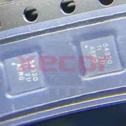
TPS70302PWPR
LDO Voltage Regulators 1A/2A Dual-Output
| 数量 | 単価(USD) | 合計金額 |
|---|---|---|
| 1 | $4.398 | $4.40 |
| 10 | $3.845 | $38.45 |
| 30 | $3.518 | $105.54 |
| 100 | $2.943 | $294.30 |
| 500 | $2.790 | $1,395.00 |
| 1000 | $2.721 | $2,721.00 |
在庫:7,592
- 90日間のアフター保証
- 365日の品質保証
- 正規品保証
- 7*24時間サービス検疫
-
部品番号 : TPS70302PWPR
-
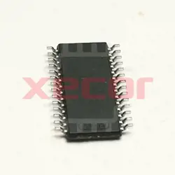
パッケージ/ケース : HTSSOP-24
-
ブランド : TI
-
コンポーネントのカテゴリ : Linear & low-dropout (LDO) regulators
-
日付シート : TPS70302PWPR データシート (PDF)
概要 TPS70302PWPR
The TPS703xx family of devices is designed to provide a complete power management solution for TI DSP, processor power, ASIC, FPGA, and digital applications where dual output voltage regulators are required. Easy programmability of the sequencing function makes this family ideal for any TI DSP application with power sequencing requirements. Differentiated features, such as accuracy, fast transient response, SVS supervisory circuit (power-on reset), manual reset inputs, and enable function, provide a complete system solution.
The TPS703xx family of voltage regulators offers very low dropout voltage and dual outputs with power up sequence control, designed primarily for DSP applications. These devices have low noise output performance without using any added filter bypass capacitors, and are designed to have a fast transient response and be stable with 47 µF low ESR capacitors.
These devices have fixed 3.3 V/2.5 V, 3.3 V/1.8 V, 3.3 V/1.5 V, 3.3 V/1.2 V, and adjustable voltage options. Regulator 1 can support up to 1 A, and regulator 2 can support up to 2 A. Separate voltage inputs allow the designer to configure the source power.
Because the PMOS pass element behaves as a low-value resistor, the dropout voltage is very low (typically 160mV on regulator 1) and is directly proportional to the output current. Additionally, since the PMOS pass element is a voltage-driven device, the quiescent current is very low and independent of output loading (maximum of 250 µA over the full range of output current). This LDO family also features a sleep mode; applying a high signal to EN (enable) shuts down both regulators, reducing the input current to 1 µA at TJ = +25°C.
The device is enabled when the EN pin is connected to a low-level input voltage. The output voltages of the two regulators are sensed at the VSENSE1 and VSENSE2 pins respectively.
The input signal at the SEQ pin controls the power-up sequence of the two regulators. When the device is enabled and the SEQ terminal is pulled high or left open, VOUT2 turns on first and VOUT1 remains off until VOUT2 reaches approximately 83% of its regulated output voltage. At that time VOUT1 is turned on. If VOUT2 is pulled below 83% (that is, in an overload condition) of its regulated voltage, VOUT1 is turned off. Pulling the SEQ terminal low reverses the power-up order and VOUT1 is turned on first. The SEQ pin is connected to an internal pull-up current source.
For each regulator, there is an internal discharge transistor to discharge the output capacitor when the regulator is turned off (disabled).
The PG1 pin reports the voltage condition at VOUT1. The PG1 pin can be used to implement an SVS (POR, or power-on reset) for the circuitry supplied by regulator 1.
The TPS703xx features a RESET (SVS, POR, or power-on reset). RESET is an active low, open drain output and requires a pull-up resistor for normal operation. When pulled up, RESET goes to a high impedance state (that is, logic high) after a 120 ms delay when all three of the following conditions are met. First, VIN1 must be above the undervoltage condition. Second, the manual reset (MR) pin must be in a high impedance state. Third, VOUT2 must be above approximately 95% of its regulated voltage. To monitor VOUT1, the PG1 output pin can be connected to MR1 or MR2. RESET can be used to drive power-on reset or a low-battery indicator. If RESET is not used, it can be left floating.
Internal bias voltages are powered by VIN1 and require 2.7V for full functionality. Each regulator input has an undervoltage lockout circuit that prevents each output from turning on until the respective input reaches 2.5 V.
主な特長
- Dual Output Voltages for Split-Supply Applications
- Independent Enable Functions (See Part Number TPS704xx
for Independent Enabling of Each Output) - Output Current Range of 1 A on Regulator 1 and 2A on Regulator 2
- Fast Transient Response
- Voltage Options: 3.3 V/2.5 V, 3.3 V/1.8 V, 3.3 V/1.5 V, 3.3 V/1.2 V,
and Dual Adjustable Outputs - Open Drain Power-On Reset with 120 ms Delay
- Open Drain Power Good for Regulator 1
- Ultralow 185 µA (typ) Quiescent Current
- 2 µA Input Current During Standby
- Low Noise: 78 µVRMS Without Bypass Capacitor
- Quick Output Capacitor Discharge Feature
- Two Manual Reset Inputs
- 2% Accuracy Over Load and Temperature
- Undervoltage Lockout (UVLO) Feature
- 24-Pin PowerPAD™ TSSOP Package
- Thermal Shutdown Protection
PowerPAD is a trademark of Texas Instruments.
All other trademarks are the property of their respective owners.
仕様
以下は、選択された部品の特性やカテゴリーに関する基本的なパラメータである。
| Output options | Adjustable Output, Dual output, Fixed Output | Iout (max) (A) | 1 |
| Vin (max) (V) | 6 | Vin (min) (V) | 2.7 |
| Vout (max) (V) | 5.5 | Vout (min) (V) | 1.2 |
| Fixed output options (V) | 1.2, 1.5, 1.8, 2.5, 3.3 | Noise (µVrms) | 78 |
| Iq (typ) (mA) | 0.185 | Thermal resistance θJA (°C/W) | 30.9, 32 |
| Rating | Catalog | Load capacitance (min) (µF) | 22 |
| Regulated outputs (#) | 2 | Features | Enable, Output discharge, Power good, Sequencing and monitoring |
| Accuracy (%) | 2 | PSRR at 100 KHz (dB) | 22 |
| Dropout voltage (Vdo) (typ) (mV) | 160 | Operating temperature range (°C) | -40 to 125 |
保証と返品
保証、返品、および追加情報
-
QAと返品ポリシー
部品の品質保証: 365 日
返品・返金:90日以内
返品・交換:90日以内
-
配送と梱包
配送: たとえば、FedEx、SF、UPS、または DHL.UPS、または DHL。
部品のパッケージング保証: 100% ESD 帯電防止保護を特徴とする当社のパッケージングには、高い靭性と優れた緩衝機能が組み込まれています。
-
支払い
たとえば、VISA、MasterCard、UnionPay、Western Union、PayPal などのチャネルです。
特定の支払いチャネルの好みや要件がある場合は、当社の営業チームにご連絡ください。
類似商品
TPS54320RHLR
Efficient 3A synchronous step-down converter with a wide input voltage range of 4.5V to 17V"
TPS54618RTER
SWIFT technology employed for efficient voltage regulation
TPS57060QDGQRQ1
Wide input voltage range for versatile use in automotive systems
TPS57040QDRCRQ1
Conv DC-DC 3.5V to 42V Synchronous Step Down Single-Out 0.8V to 39V 0.5A Automotive AEC-Q100 10-Pin VSON EP T/R
TPS57160QDRCRQ1
IC for regulating voltage down to desired levels with 1.5A current capability
TPS23861PW
Quad LAN POE PSE Controller with Power Switch Technology
TPS27S100APWPR
Buffer and inverter-based peripheral driver with a 7A capacity in a PDSO14 package
TPS60150DRVR
Charge pump with a 2x2 SON footprint that outputs 5V at 140mA